One big wire change from 1997 still helping chips achieve tiny scale

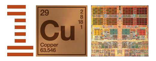
The IT state-of-the-art 20 years ago was rapidly ending, and we – and I mean everyone in the industry that made a device with a chip inside of it – needed something new to keep up with the demand for ever-faster, better electronics. These were the days of laptops with 233 MHz speeds, and Deep Blue was exploring a mere 200 million possible chess positions per second. Without one element in the eleventh group of the periodic table, Cu, our computers and devices would not have advanced much beyond the speed and power of two decades ago.
The teams I alternately partnered with and led between IBM Research, and IBM's Semiconductor R&D Center discovered how to replace the aluminum wires that connected the transistors and various parts of a computer chip with Cu – copper. Aluminum on-chip wiring had maybe one or two more nodes to go before its performance would have hit a metaphorical brick wall. That means our mainframe supercomputers would have topped out at 0.18 μm (180 nanometers) node chips. And the trickledown effect to present day would have left us with computers stuck at late 90s speed and performance, and cellphones would never have gotten smart.
Copper conducts electricity significantly better than aluminum, and also handles higher current densities without wearing out. By the 1980s, IBM believed copper was the next, best option for improving chip power, performance, and reliability, even if the rest of the industry wasn't convinced. The challenges were one, how to fabricate copper interconnects; and two, how to overcome "copper poisoning" – the concern that copper could damage chips, or the entire manufacturing facility, if it came into contact with silicon transistors.
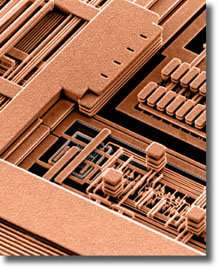
Preliminary research by my IBM colleagues C-K Hu, Cyprian Uzoh, Frank Kaufman, and Barbara Luther showed in their 1993 paper, "Planar Copper Polyimide Back End Of The Line Interconnections For ULSI Devices," that multilevel copper wires could be fabricated. Their innovative electroplating to deposit copper; their damascene scheme (the layering of different metals into an etched pattern on a chip) to pattern copper; and the barriers they developed for copper containment were seminal developments that, while not manufacturable technology, and not connected to transistors yet, put us on a path to aluminum replacement.

This triple solution of electroplating, damascene, and diffusion barriers proved superior to anything else being tried at the time. As a side benefit, electroplated copper's "magic" trace impurities also improved its reliability. I firmly believe we discovered these superior, cheaper, and easier(!) options before anyone else because of IBM Research's multi-disciplinary expertise across chemistry, electrical engineering, physics, chip packaging, and manufacturing. It was only fitting that Uzoh, the chemist on the team, whose name in his native Nigerian language means "copper," came up with the electroplated copper recipe.
Dual-damascene puts copper in working chips
Proving that copper might work as the multi-level on-chip wiring was a major step forward. But until we could connect them in a working chip, and fix weaknesses to pass all IBM's CMOS qualification criteria, our colleagues on the development and manufacturing side were not interested. In particular, Luther et al's. single damascene copper was deemed non-manufacturable, from yield, reliability, and cost standpoints.
Upon hearing this negative pronouncement, and in the interest of meeting true CMOS production requirements, I launched a side-project to prove a copper solution could work on actual microprocessors. And my team reengineered the plating, patterning, and barrier recipe with a dual damascene process – essentially adding silicon dioxide (glass) as a protective layer at the same time the copper wires are added to a chip's trenches.
By 1995, our new dual damascene process was producing quality data points that passed product-level quality tests for deposition, patterning, containment, packaging, and preliminary CMOS integrated circuit stress tests. Our colleagues in development and manufacturing not only took notice, but committed to insert copper into our fabs, and conduct a full production qualification course for our next-generation microprocessors. After two more years of development and qualification, IBM announced a manufacturable copper-CMOS technology in September of 1997.
By 1998, IBM PowerPC chips went from an aluminum-powered 300 MHz, to a copper-boosted 400 MHz – a 33 percent speed improvement.
Electronic life after Copper
Copper will always have its place in the majority of future on-chip micro- and nano-scale wiring at 15 nm. But below that, new metals will have to come into play to keep up with Moore's Law of shrinking cheaper transistors on chips. These metals must have higher intrinsic resistivity than copper. These metals' small nanowires may still beat copper for net resistance by eliminating the need for a diffusion barrier, and reducing electron scattering effects. Some potential candidates include ruthenium, cobalt, nickel, and other platinum-group noble metals.
I will be talking about copper's inception and legacy, as well as its potential future scenario at the IEEE's Nanotechnology Symposium in Albany, NY this month, as well as delivering an invited talk titled "20 Years of Cu BEOL in Manufacturing, and its Future Prospects" at the December IEEE International Electron Devices Meeting conference in San Francisco.
Provided by IBM


